← Back to Projects

Embedded Systems · Sensor Fusion · RF

Navigation Board PCB In Progress

STM32F411 GNSS 9DOF IMU nRF24L01 6-Layer PCB USB-C Power

A custom 6-layer navigation board integrating GNSS, inertial sensing, and wireless communication into a compact embedded system. The board estimates real-time vehicle attitude using a Kalman filter that fuses GPS and IMU data, transmitting results wirelessly to a host computer for visualization.

Navigation Board PCB

Specifications

At a Glance

MCU
STM32F411CEU6
GNSS
u-blox NEO-M9N
IMU
9DOF (Accel + Gyro + Mag)
RF Link
nRF24L01
Power
LiPo + USB-C Charging
PCB
6-layer, impedance controlled

System Architecture

Data Flow

GNSS
NEO-M9N
+
IMU
9DOF
→
STM32F411
Sensor Fusion
→
nRF24L01
RF Link
→
Host PC
Python Viz
Goal: Fuse absolute positioning (GNSS) with high-rate inertial data (IMU) using a Kalman filter to estimate real-time orientation and motion, then stream state estimates wirelessly to a host computer for visualization.

Design Overview

Hardware + Firmware

This board was designed as a dedicated navigation and state estimation platform. The hardware is complete and functional, integrating all sensing, processing, and communication subsystems onto a single PCB.

Hardware Integration

The design centers around the STM32F411 MCU, which interfaces with the NEO-M9N GNSS receiver over UART for global positioning, and a 9DOF IMU over SPI/I2C for high-rate motion sensing. The nRF24L01 provides a low-latency 2.4 GHz RF link to stream processed state estimates to an external computer.

Power System

The board is powered by a single-cell LiPo battery with onboard USB-C charging circuitry. Independent regulation stages supply stable rails for the RF front-end, digital logic, and analog sensing paths, minimising noise coupling into sensitive IMU measurements.

PCB Stackup

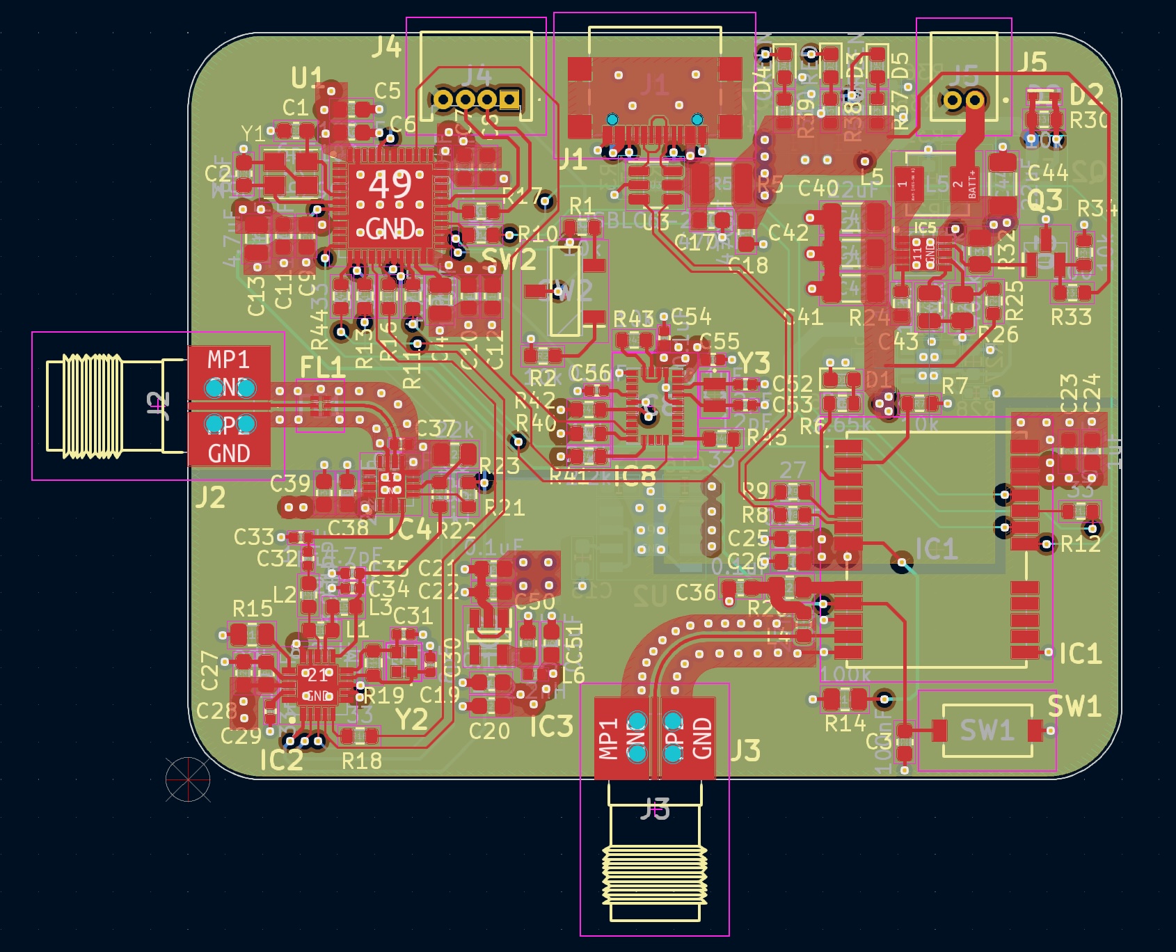
A 6-layer stackup was chosen to provide controlled impedance for RF and GNSS antenna traces, solid ground referencing across all layers, and clean power distribution. Dedicated power and ground planes minimise EMI and improve signal integrity throughout.
Schematic

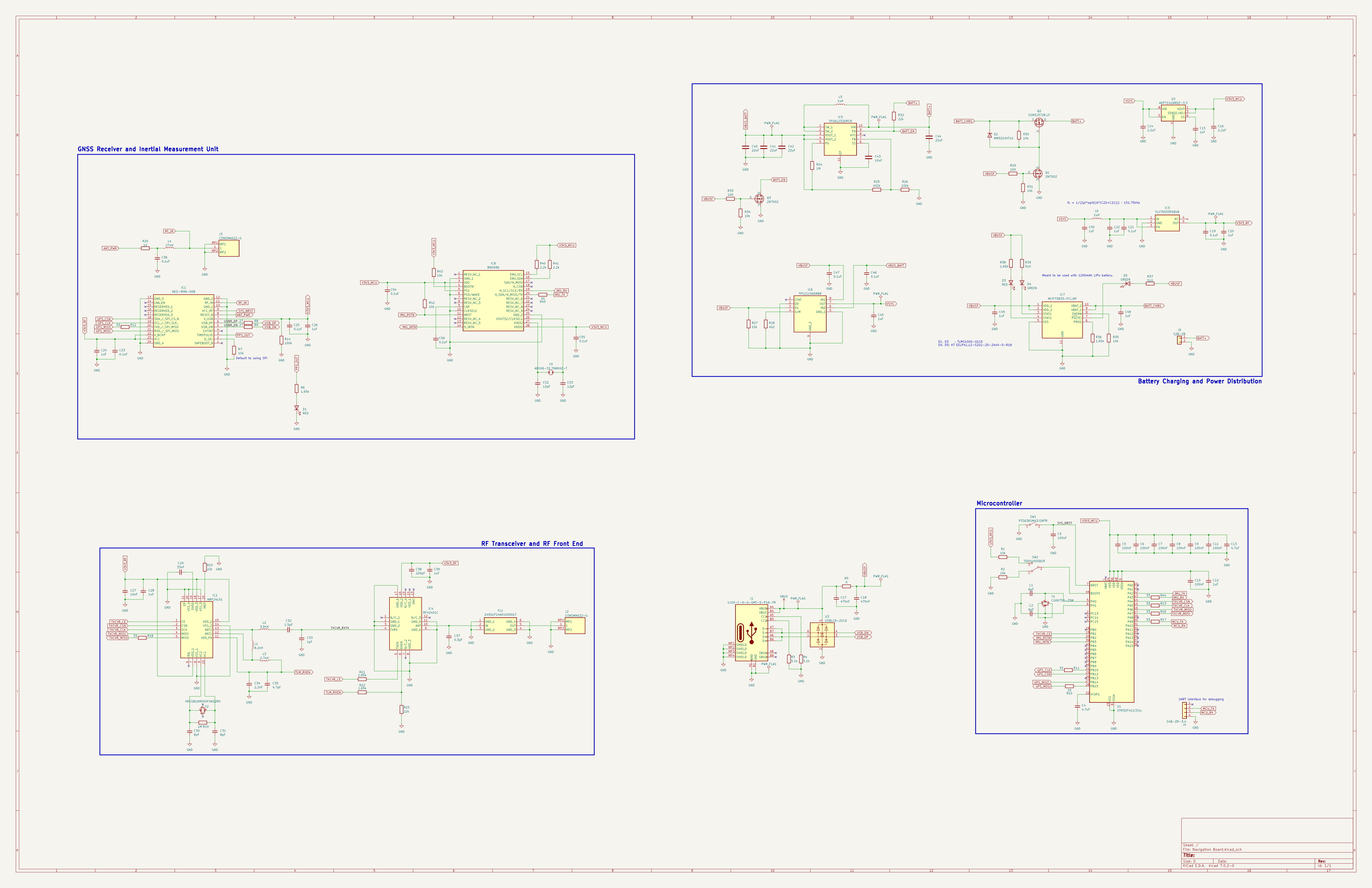
Full Circuit Diagram

RF, digital, and power sections are grouped accordingly. Separate power supply for RF components for better isolation form noise.

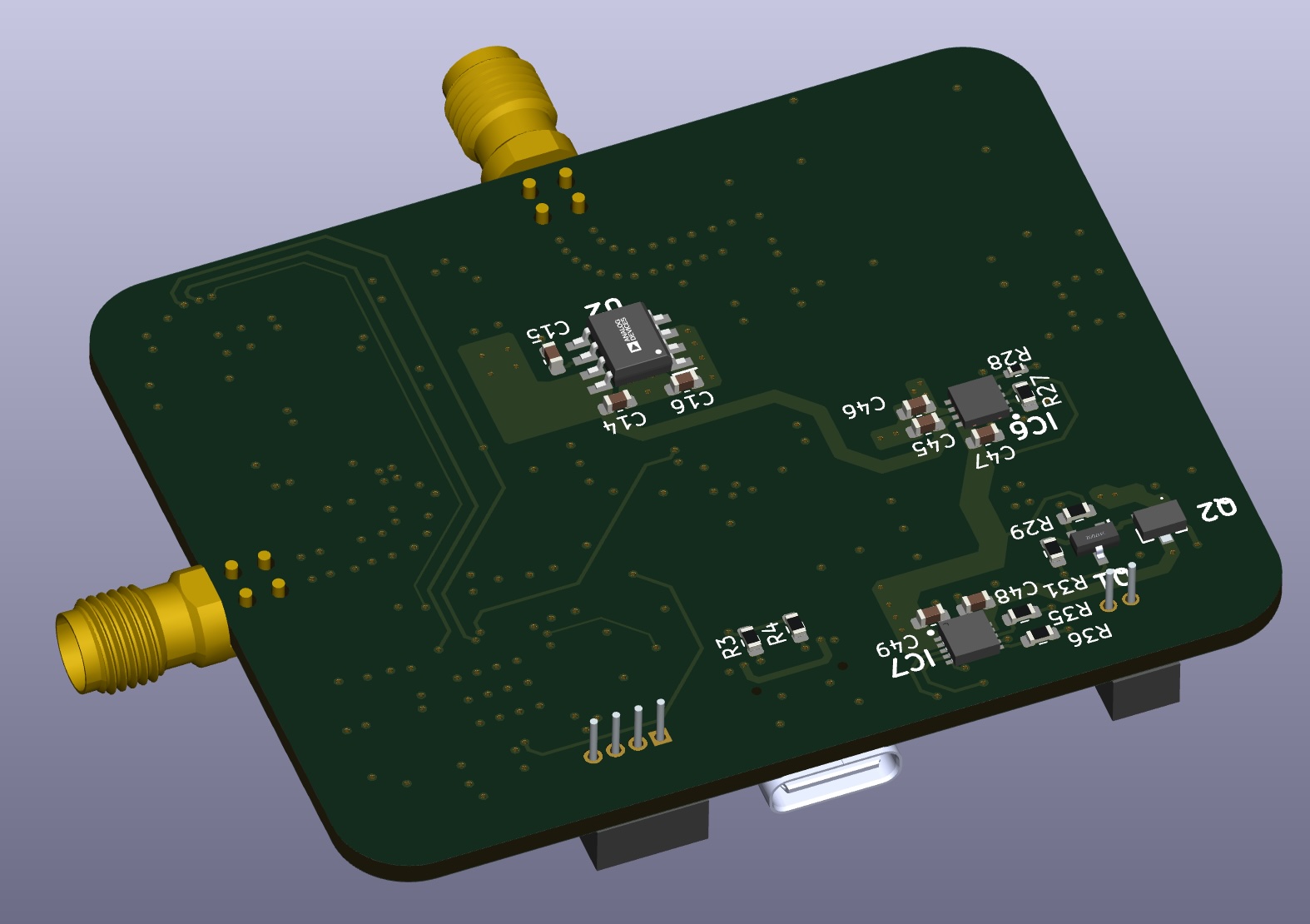
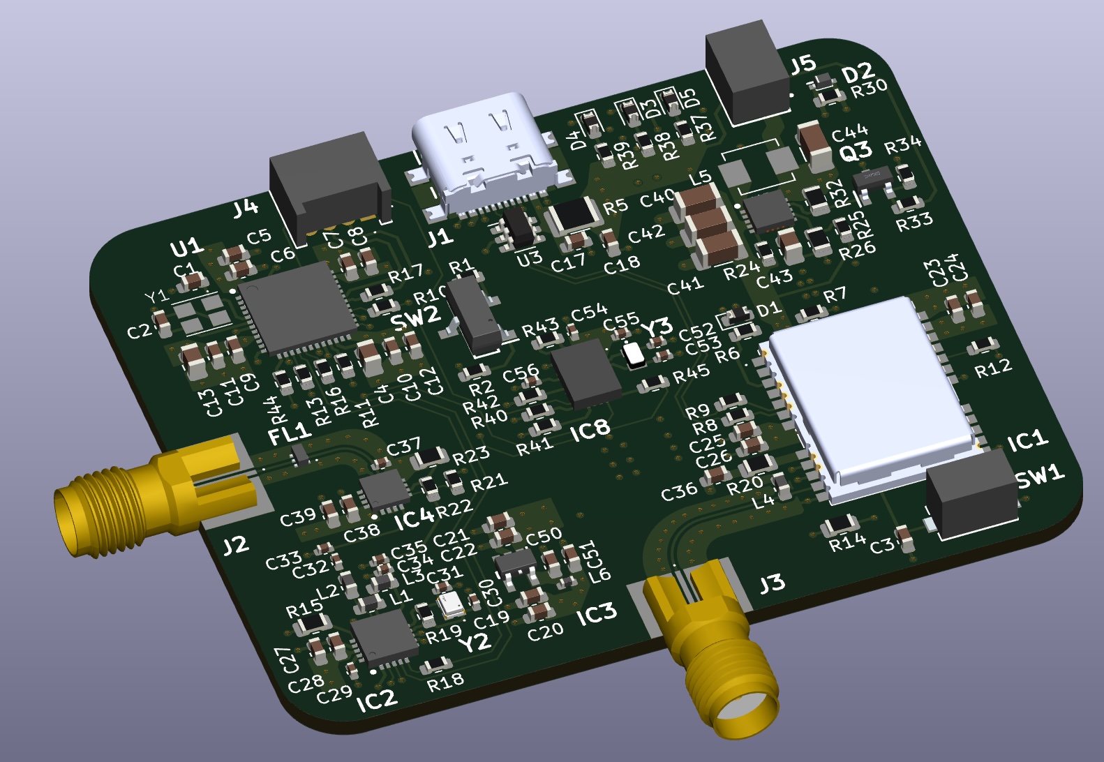
PCB Layout & 3D Model

KiCAD Design Files

PCB Stackup

Layer Details — Design Spreadsheet

nav_board_stackup.xlsx
Google Sheets

Next Steps

Kalman Filter Implementation

The hardware platform is complete. The main focus moving forward is implementing a robust Kalman filter for sensor fusion and the accompanying host-side visualization pipeline.