Design Process
From Simulation to Board
This project started as a way to practice playing guitar late at night without
bothering anyone. The requirement was simple: low noise, flat frequency response
across the audible band, and enough drive current to push a pair of headphones
to a comfortable volume.
Op Amp Selection — LM358 vs NE5532
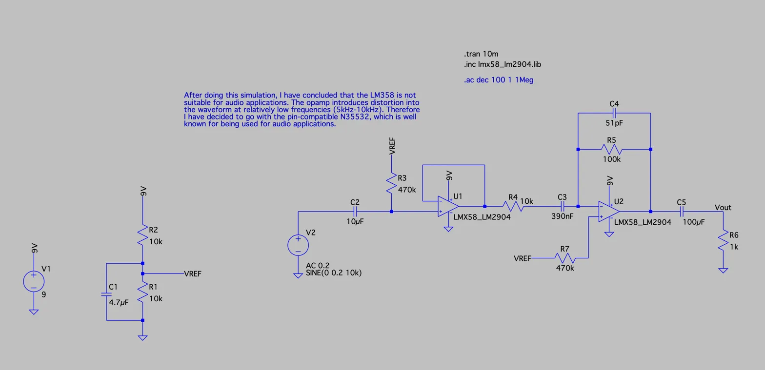
The initial design used the common LM358 dual op amp. Running LTSpice transient
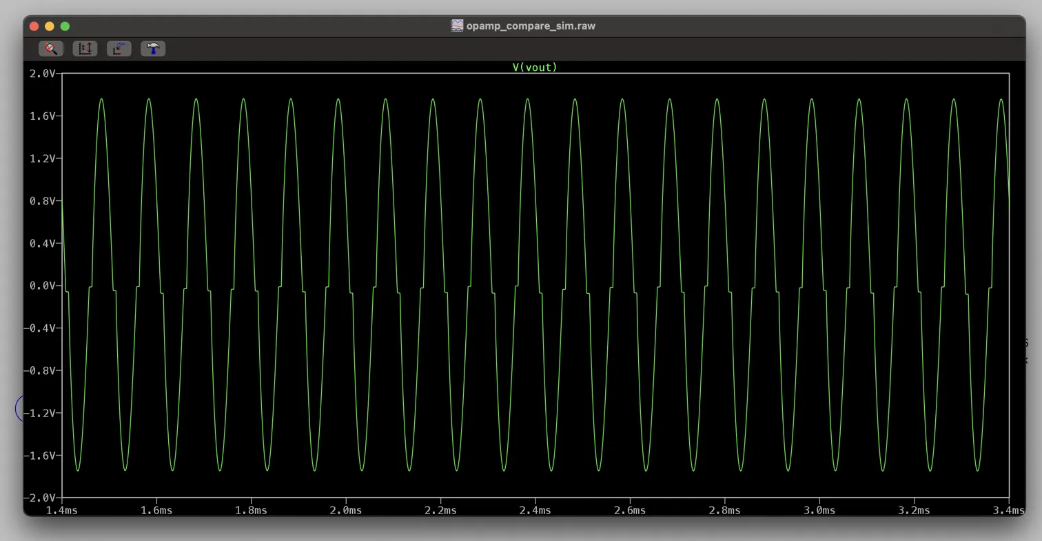
and AC simulations quickly revealed a serious problem: the LM358 introduces
noticeable crossover distortion at frequencies as low as 5–10 kHz — well within
the audible range and far too early for an audio application. The simulated output
waveform showed characteristic "notching" near the zero crossing at mid-to-high audio frequencies.
Key Finding: The LM358's output stage is optimized for DC and low-frequency
work. Its limited slew rate and crossover distortion make it a poor choice for audio paths.
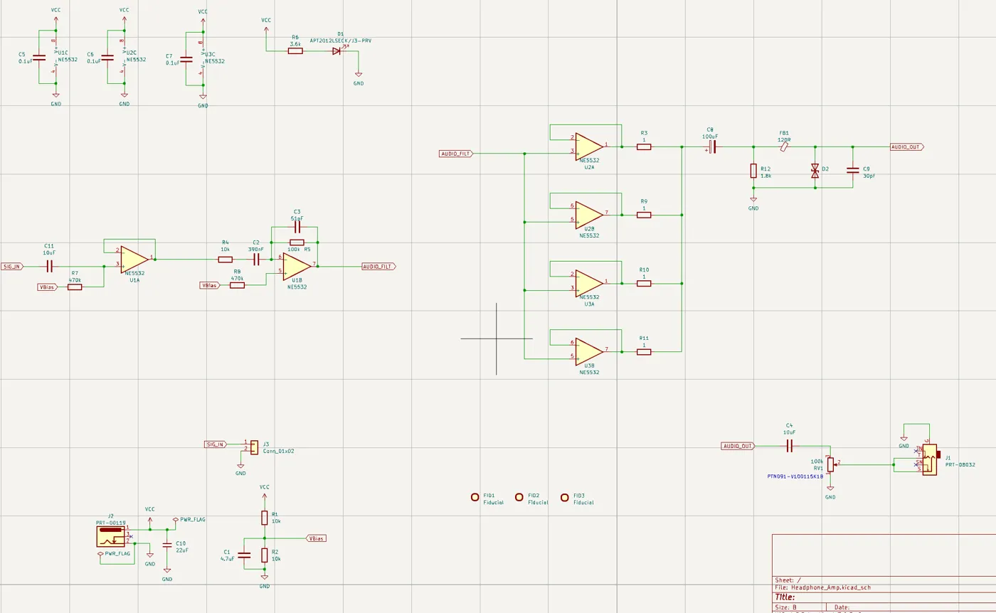
The pin-compatible NE5532 is an industry-standard audio op amp with
dramatically better noise performance (5 nV/√Hz) and far higher slew rate, solving both problems.
Paralleling Output Stages
Headphones present a relatively low impedance load (~32Ω typical). Rather than
use a discrete output buffer transistor stage, four NE5532 op amp sections
are wired in parallel at the output. This multiplies the available output current
by four while averaging out individual op amp noise — a clean way to get more drive
without adding complexity or BJT-related design headaches.
PCB Layout
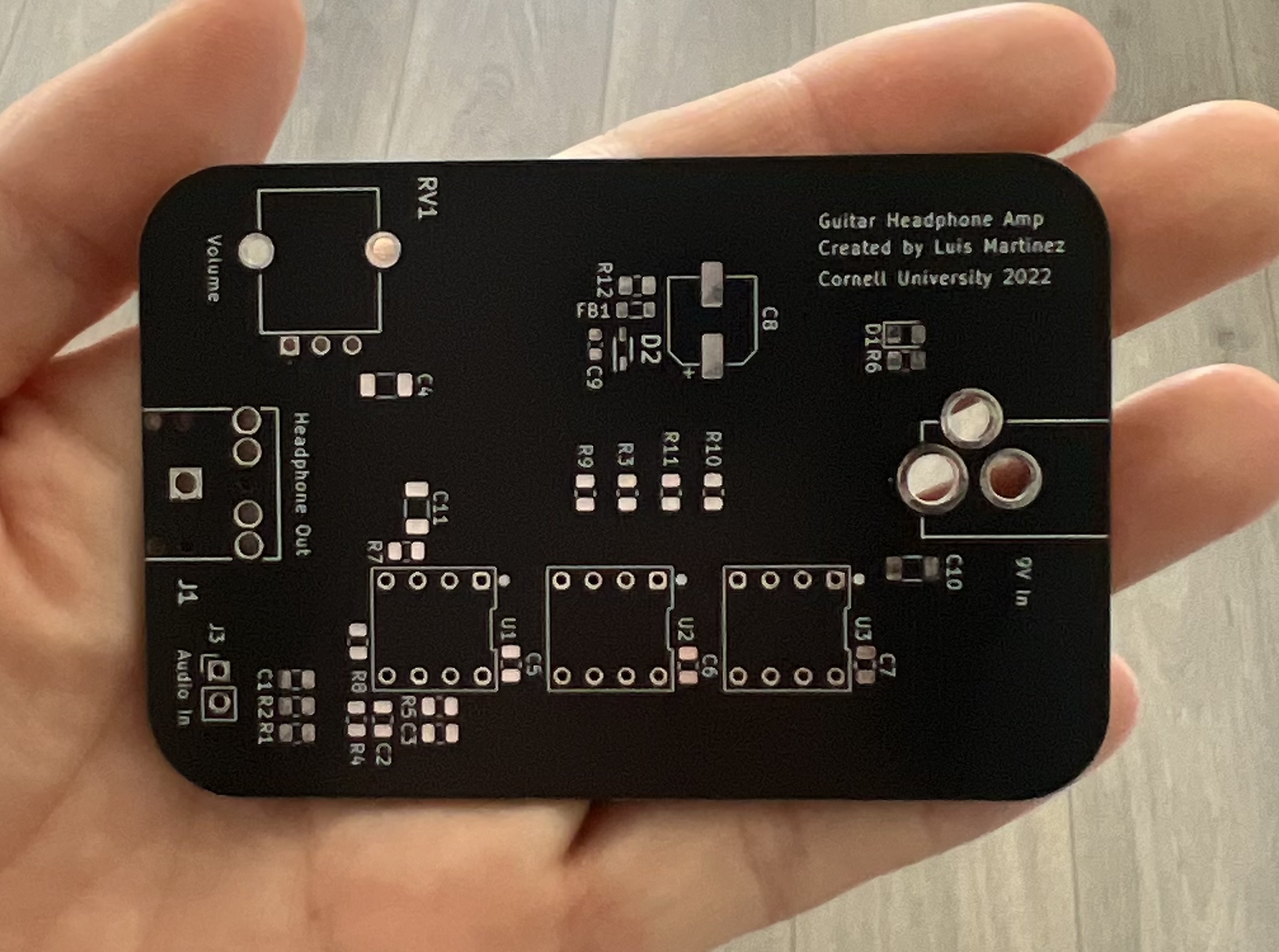
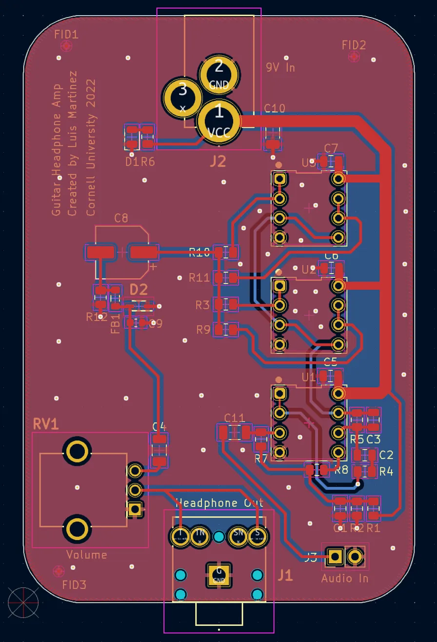
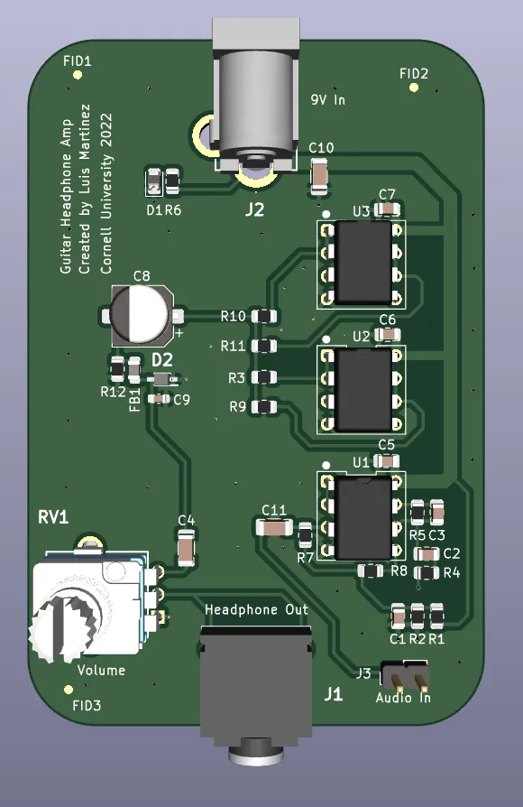
The 2-layer board was laid out in KiCAD. Power and ground planes on the back copper
help with noise rejection. Decoupling caps are placed directly at each op amp supply pin.
A ferrite bead (FB1) and protection diode (D2) guard the audio output. The barrel jack,
potentiometer, and both audio jacks are positioned at the board edges for easy panel mounting.